Synopsys certifies design flows on TSMC's A14
Chip designers can now take Synopsys tools all the way to signoff on TSMC's A14 process, the company says, with agentic AI handling more of the fiddly work.
Synopsys says its design tools are now certified for A14, TSMC's next-generation process, in a release published on 23 September. Certification covers both digital and analog flows, which means a chip team can run a project from implementation through to signoff on the node using one toolchain rather than stitching together several.
Agentic AI moves into the design flow
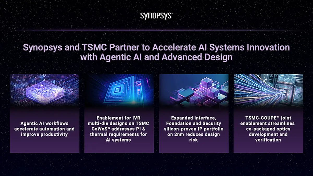
The release leans hard on automation. Synopsys says it is working with TSMC on agentic AI capabilities that take over parts of analog, digital and multi-die design work, with LLM-assisted analysis inside Fusion Compiler and a new chiplet floorplan flow built on its 3DIC Compiler platform that automates floorplanning for designs using TSMC's 3DFabric packaging. On the analog side the two companies report device routing enablement on A14, the step that makes place-and-route automation usable on advanced nodes.
Power delivery and optics
Two items stand out for anyone tracking AI datacentre silicon. Synopsys says its 3DIC Compiler can now co-design and simulate integrated voltage regulators on TSMC's CoWoS packaging, and IVRs are one of the levers for holding power integrity together as accelerator packages draw more current. The company also says it continues to work with TSMC on co-packaged optics design on the COUPE platform, through a flow that spans 3DIC implementation, multiphysics analysis and optimisation.
The IP checklist
Synopsys also lists IP milestones reached on TSMC's N2P process, including PCIe 7.0, HBM4, LPDDR6, LPDDR5X and LPDDR5, a 224G Ethernet PHY, UCIe, one-time-programmable memory and process, voltage and temperature monitoring IP. Michael Buehler-Garcia, a senior vice president at Synopsys, said the joint work addresses "the continuum of silicon to systems co-design capabilities needed to accelerate development of next-generation AI and high-performance computing systems". Aveek Sarkar of TSMC said certified design tools and silicon-proven IP, combined with TSMC's process and packaging work, let customers "push the boundaries of performance, integration, and energy efficiency".
Our opinion
Tool certification is the least glamorous news in the semiconductor calendar and one of the few items that genuinely gates a node's economics. A14 is not much use to TSMC if every customer has to invent a tape-out flow for it, so the interesting claim here is not the process but the handshake: two companies agreeing that implementation and signoff both work, analog included. Analog is the tell, because it is the part of chip design that has resisted automation longest and the part that decides whether an AI accelerator's power delivery survives contact with a datacentre. The agentic AI framing deserves more scepticism than the certification does. Automation that shortens floorplanning is useful engineering; calling it agentic is marketing, and no design team will accept an LLM's signoff without a human reading the corner cases first.