Intel says it has processed one million High-NA EUV wafers as chipmaking race accelerates
Intel says it has processed more than one million wafers using High-NA EUV equipment, while a new Intel Foundry and ASML collaboration aims to accelerate the technology’s production readiness.
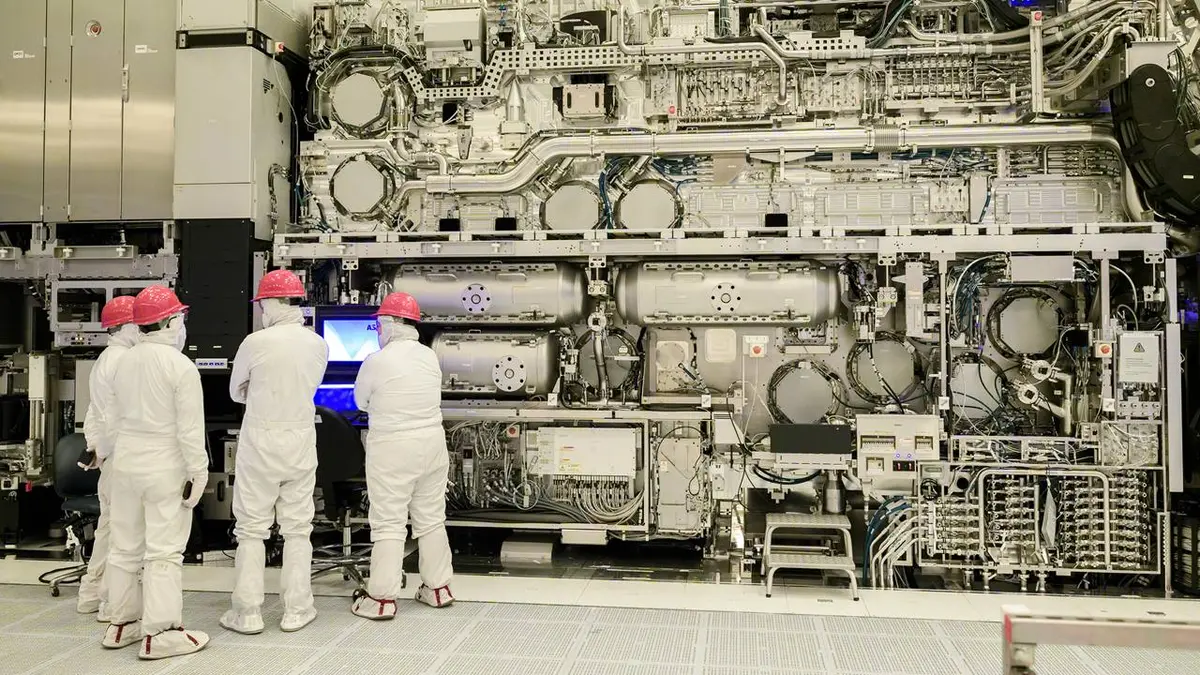
Intel says it has processed more than one million wafers using High-NA EUV equipment, while a new Intel Foundry and ASML collaboration aims to accelerate the technology’s production readiness.
Intel and ASML announced a High-NA EUV production milestone, with Intel saying it has processed more than one million wafers using the equipment. Tom’s Hardware reports that Intel also claims this exceeds the rest of the industry combined.
The reporting further describes work on large 6×12 photomasks intended to improve production speed and reduce costs. Those mask details and the “more than the rest of the industry combined” comparison should be treated as Intel or secondary-report claims rather than independent production measurements.
Why it matters
High-NA EUV is designed to print smaller and more complex chip features with fewer process steps, but the equipment is expensive and difficult to integrate into high-volume manufacturing. Reaching a wafer milestone is useful evidence of progress; it is not the same thing as proving cost-effective commercial production.
Our opinion
This is the sort of manufacturing milestone that matters long before consumers see a product label change. Intel needs High-NA EUV to become boring, repeatable factory infrastructure, not merely an impressive demonstration. The wafer count is encouraging, but yield, throughput and customer adoption will decide whether it becomes a competitive advantage.